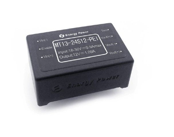
DC-DC Converters 13W Output 12V MT13-24S12-PEI
Key Features
Output power: 13W
Wide input range:18-36Vdc
High conversion efficiency: 88%
Line regulation to ±0.5%
Load regulation to ±0.5%
Isolation voltage :1,500V
Enable (ON/OFF) control
Output over-current protection
Hiccup mode short circuit protection
Over-temperature protection
Input under-voltage lock-out
Output voltage trim -5~+10 % Vout
Product Overview
These DC-DC converter modules use advanced power processing, control and packaging technologies to provide the performance, flexibility, reliability and cost effectiveness of a mature power component. High frequency Active Clamp switching provides high power density with low noise and high efficiency.
1. Electric Characteristics
1.1 Absolute Maximum Ratings
| Parameter |
Min |
Typ |
Max |
Units |
Notes |
| Input Voltage |
|
|
45 |
Vdc |
Continuous, non-operating |
| |
|
36 |
Vdc |
Continuous, operating |
| |
|
45 |
Vdc |
Operating transient protection,<100mS |
| Isolation voltage |
|
|
2000 |
Vdc |
Input to output |
| Operating Temperature |
-20 |
|
85 |
℃ |
In view of PCB Temperature |
| Storage Temperature |
-30 |
|
95 |
℃ |
|
| Enable to Vin- Voltage |
-0.3 |
|
10 |
Vdc |
|
1.2 Input Characteristics
| Parameter |
Min |
Typ |
Max |
Units |
Notes |
| Input Voltage Range |
18 |
24 |
36 |
Vdc |
|
| Under-Voltage Lockout |
|
17 |
17.5 |
Vdc |
Recovery point |
| 16 |
16.5 |
|
Vdc |
Protect point |
| Maximum Input Current |
|
|
0.9 |
A |
Input Vin min,Output full load |
| Efficiency |
|
88 |
|
% |
Rated Input;Rated Load |
| Dissipation,standby |
|
0.3 |
|
W |
No Load |
1.3 Output Characteristics
| Parameter |
Min |
Typ |
Max |
Units |
Notes |
| Output Voltage Set Point |
11.85 |
12.00 |
12.15 |
Vdc |
Nominal input. No Load |
| Output Voltage Range |
11.75 |
12.00 |
12.25 |
Vdc |
|
| Output Current Range |
0.01 |
|
1.1 |
A |
|
| Line Regulation |
|
±0.02 |
±0.5 |
% |
|
| Load Regulation |
|
±0.02 |
±0.50 |
% |
|
| Current Limit |
1.15 |
1.4 |
1.70 |
A |
Output voltage 95% of nominal |
| Short Circuit Current |
1 |
|
3 |
A |
|
| Ripple (RMS) |
|
25 |
|
mV |
Nominal input; full load; 20 MHz bandwidth. |
| Noise(Peak-to-Peak) |
|
80 |
|
mV |
| Maximum Output Cap |
|
|
3000 |
μF |
|
1.4 Dynamic Response Characteristics
| Parameter |
Min |
Typ |
Max |
Units |
Notes |
| Change In Output Current |
|
100 |
|
mV |
50% to 75% to 50% Iout max; (di/dt=0.1A/μs). |
| |
100 |
|
mV |
50% to 75% to 50% Iout max; (di/dt=0.3A/μs). |
| Dynamic recovery time |
|
200 |
|
µS |
|
| Turn-on Time |
|
2 |
|
mS |
Starting from vin to vout rise to 90% |
| Turn-off overshoot |
|
2 |
|
% |
|
1.5 Functional Characteristics
| Parameter |
Min |
Typ |
Max |
Units |
Notes |
| Switching Frequency |
180 |
200 |
250 |
KHz |
|
| Output Voltage Trim |
|
|
10 |
% Vout |
Trim Up |
| |
|
5 |
Trim Down |
| Enable Voltage |
|
|
0.5 |
mA |
|
|
Enable (ON/OFF) Control
Positive Logic
|
2.5 |
|
10 |
Vdc |
ON-Control, Logic high or floating |
| 0 |
|
1.5 |
Vdc |
OFF-Control, Logic low |
| Over-Load Protection |
105 |
130 |
150 |
% |
Current mode,Pulsecurrent(100% raredload) |
| Short-Circuit Protection |
|
|
65 |
mΩ |
Hiccup mode,since the recovery |
| Over-Temperature Protection |
|
105 |
|
℃ |
Type: Non-Latching, Auto-Recovery;Threshold, PCB Temperature |
| |
90 |
|
℃ |
Recovery point |
1.6 Isolation Characteristics
| Parameter |
Min |
Typ |
Max |
Units |
Notes |
| Isolation Voltage |
1500 |
|
|
Vdc |
Input to Output |
| 1500 |
|
|
Vdc |
In to base |
| 500 |
|
|
Vdc |
Out to base |
| Isolation Resistance |
10 |
|
|
MΩ |
At 500VDC to test it when atmosphericpressure and R.H. is 90% |
| Isolation Capacitance |
|
1000 |
|
pF |
|
2. General Characteristics
| Parameter |
Min |
Typ |
Max |
Units |
Notes |
| Weight |
|
20 |
|
g |
|
| MTBF ( calculated ) |
1 |
|
|
MHrs |
TR-NWT-000332;80% load,300LFM, 40℃ Ta |
3. Environmental Characteristics
| Parameter |
Min |
Typ |
Max |
Units |
Notes |
| Operating Temperature |
-20 |
|
85 |
℃ |
Base PCB temperature |
| Storage Temperature |
-30 |
|
95 |
℃ |
Ambient temperature |
| Temperature Coefficient |
|
|
±0.02 |
%/℃ |
|
| Humidity |
20 |
|
95 |
%R.H. |
|
4. Standards Compliance
| Parameter |
Notes |
| MIL-STD-704 |
|
| MIL-STD-1399 |
|
| MIL-STD-810 |
|
| UL/cUL60950 |
|
| EN60950 |
|
| GB4943 |
|
| IEC 61000-4-2 |
|
5. Typical Wave And Curves

Figure 1: Efficiency at nominal output voltage vs.load current for minimum, nominal, and maximuminput voltage at 25°C.
Figure 2: Efficiency at nominal output voltage and60% rated power vs. airflow rate for ambient airtemperatures of 25°C.
Figure 3: Maximum output power derating curves vs.ambient air temperature for airflow rates of 0 LFM through400 LFM with air flowing from pin 1 to pin 3 (nominalinput voltage).
Figure 4: Output voltage ripple at nominal inputvoltage and rated load current (20 mV/div). Loadcapacitance: 0.1μF ceramic capacitor and 10μFtantalum capacitor. Bandwidth: 20 MHz.
Figure 5: Ambient temperature is 25 ℃, the loadcarried by the load (power 13W), the thermalimaging map.
Figure 6: Turn-on transient at full load (resistiveload) (100 ms/div).Input voltage pre-applied.Ch1:Vout (5V/div);Ch2:ON/OFF Input (5V/div)
Figure 7: Shut-down fall time at full load (2ms/div).Ch1:Vout (5V/div);Ch2:ON/OFF Input (5V/div)
Figure 8: Output voltage response to step-change inload current (50%-75%-50% of Iout(max); dI/dt =0.1A/μs). Load cap: 10μF, 100 mΩ ESR tantalumcapacitor and 1μF ceramic capacitor. Ch1: Vout(200mV/div)
Figure 9: Output voltage response to step-change inload current (50%-75%-50% of Iout(max): dI/dt =0.3A/μs). Load cap: 220μF, 30mΩ ESR tantalumcapacitor and 1μF ceramic cap. Ch1: Vout (200mV/div)
6. Physical Information
6.1 Mechanical Outline
Notes:
1. All other pins are 0.6mm dia
2. Pin4 and Pin6 are parallel connection. The user could achieve the function Vout(+) whether connect either two pin orboth.
3. Tolerances: x.xx±0.02 in. (x.x±0.5mm).x.xxx±0.010 in. (x.xx±0.25mm)
6.2 Pin Designations
| Pin No. |
Name |
Function |
| 1 |
Vin(-) |
Negative Input voltage |
| 2 |
Enable |
TTL input to turn converter on and off, referenced to Vin(-), with internal pull up. |
| 3 |
Vin(+) |
Positive Input voltage |
| 4 |
Vout(+) |
Positive Output Voltage |
| 5 |
Vout(-) |
Negative Output Voltage |
| 6 |
Vout(+) |
Positive Output Voltage |
| 7 |
Trim |
Output Voltage Trim |

 پیام شما باید بین 20 تا 3000 کاراکتر باشد!